FULL WAVE RECTIFIER
Full wave rectifier
rectifies the full cycle in the waveform i.e. it rectifies both the positive
and negative cycles in the waveform.
A full wave rectifier converts both halves of each cycle of an
alternating wave (AC signal) into pulsating DC signal.
The
full wave rectifier can be further divided mainly into following types.
1.
Center Tapped Full Wave Rectifier
2.
Full Wave Bridge Rectifier
Center Tapped Full Wave Rectifier
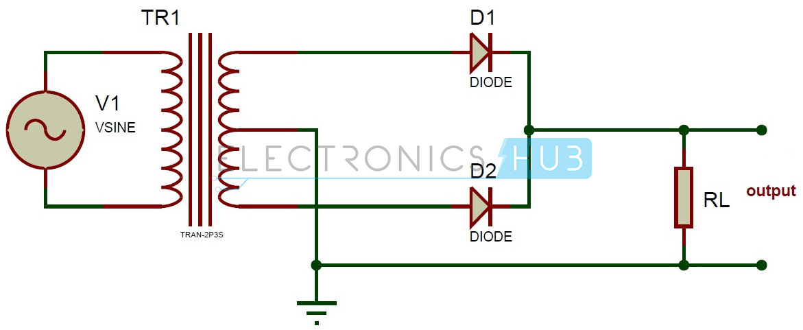
CIRCUIT DIAGRAM

CONSTRUCTION
A center-tapped full wave rectifier system consists of:
- Center-tapped Transformer
- Two Diodes
- Resistive Load
Ø In the center tapped full wave rectifier two diodes are used.
These are connected to the center tapped
secondary winding of the transformer.
Ø The positive terminal of two diodes is connected to the two
ends of the transformer.
Ø
Center tap divides the total secondary voltage
into equal parts.
Ø
Center tap is the
contact made at the middle of the winding of the transformer.
WORKING
Case 1- D1 Conduct only
ü
During positive half
cycle Diode D1 is connected to the positive terminal and D2 is connected to the
negative terminal.
ü
Thus diode D1 is in
forward bias and the diode D2 is reverse biased.
ü
Only diode D1 starts
conducting and thus current flows from diode and it appears across the load RL.
ü
So positive cycle of
the input is appeared at the load.
Case 2- D2 conduct only
ü
During the negative half cycle Diode D2 is applied with the positive cycle.
ü
D2 starts conducting
as it is in forward bias.
ü
The diode D1 is in
reverse bias and this does not conduct.
ü
Thus current flows
from diode D2 and hence negative cycle is also rectified, it appears at the
load resistor RL.
Conclusion
By comparing the current flow through
load resistance in the positive and negative half cycles, direction of the
current flow is same. Thus the frequency of rectified output voltage is two
times the input frequency. The output that is rectified is not pure, it
consists of a dc component and a lot of ac components of very low amplitudes.
PEAK INVERSE VOLTAGE
PIV is defined as the maximum
possible voltage across a diode during its reverse bias.
During the first half that is positive half
of the input, the diode D1 is forward bias and thus conducts providing no
resistance at all. Thus, the total voltage Vs appears in the upper-half of the
ac supply, provided to the load resistance R.
Similarly, in the case of diode D2 for the
lower half of the transformer total secondary voltage developed appears at the
load. The amount of voltage that drops across the two diodes in reverse bias is
given as
D2 = Vm + Vm = 2Vm
D1 = 2Vm
Vm = voltage developed across upper and lower
halves.
Full Wave Bridge Rectifier
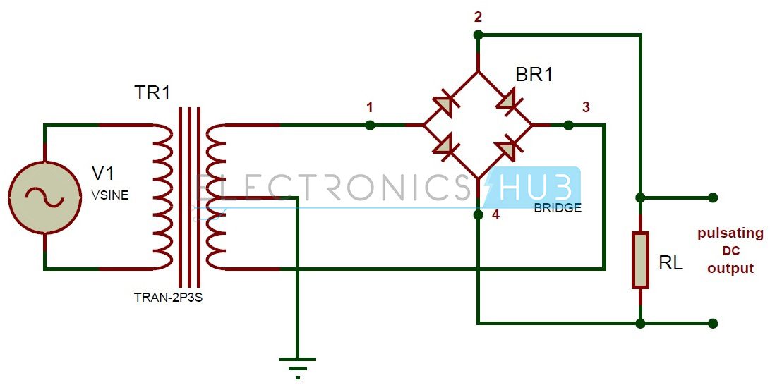
CIRCUIT DIAGRAM

A full wave bridge rectifier is a type of rectifier which will use four diodes or more than that in a bridge formation. A full wave bridge rectifier system consists of
- Four Diodes
- Resistive Load
Ø
The working of a bridge rectifier is simple.
Ø
The secondary winding of the transformer is
connected to the two diametrically opposite points of the bridge at points 1
and 3. Assume that a load is connected at the output.
Ø
The load RLoad is connected to
bridge through points 2 and 4.
WORKING
Case
1- D1, D4 Conducts
only
ü
During first half cycle, the upper portion
of the transformer secondary winding is positive with respect to the lower
portion.
ü
Thus only diodes D1 and D4 are
forward biased. Current flows through path 1-2, enter into the load RL.
It returns back flowing through path 4-3.
ü
During this half input cycle, the diodes D2 and
D3 are reverse biased.
ü
Hence there is no current flow through the path
2-3 and 1-4.
Case 2- D2, D3 Conducts only
ü
During the next cycle, lower portion of the
transformer is positive with respect to the upper portion.
ü
Thus only diodes diodes D2 and D3 are forward
biased. Current flows through the path 3-2 and flows back through the path 4-1.
ü
During this half input cycle, the diodes D1 and
D4 are reverse biased.
ü
So there is no current flow through the path 1-2
and 3-4.Thus negative cycle is rectified and it appears across the load.
PEAK INVERSE VOLTAGE
At any instant when the transformer
secondary voltage attains positive peak value Vmax, diodes D1 and D3 will be
forward biased (conducting) and the diodes D2 and D4 will be reverse biased
(non conducting).
If we consider ideal
diodes in bridge, the forward biased diodes D1 and D3 will have zero
resistance.
This means voltage drop
across the conducting diodes will be zero.Thus,
PIV of a bridge rectifier = Vmax (max of
secondary voltage)
Advantages
·
The ripple frequency
is two times the input frequency.
·
Efficiency is higher.
·
Ripple factor is less.
·
Higher output voltage.
·
Higher transformer
utilization factor.
·
Utilizes both halves
of the AC waveform.
Disadvantages
·
More expensive than
half-wave rectifier.
·
It requires more
diodes, two for center tap rectifier and four for bridge rectifier.
·
PIV rating of the
diode is higher.
Video Animation
No comments:
Post a Comment